Difference between revisions of "826 ADC"
(→Measuring isolated sources) |
(→Measuring isolated sources) |
||
| Line 9: | Line 9: | ||
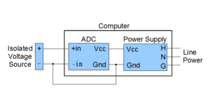
[[File:AdgGroundReference.gif|thumb|300px|To prevent measurement errors, connect unreferenced sources to the J1 GND signal, either directly or through a resistor]] | [[File:AdgGroundReference.gif|thumb|300px|To prevent measurement errors, connect unreferenced sources to the J1 GND signal, either directly or through a resistor]] | ||
| − | Measurement accuracy can be significantly degraded if an | + | Measurement accuracy can be significantly degraded if an AIN is connected to an unreferenced voltage source such as a battery or isolated power supply, or a sensor powered by such sources. Since the source is isolated, the AIN has no current return to GND and consequently the input signal may be pulled (by protection circuitry) beyond the maximum allowed CMV. The resulting measurement errors can manifest in various ways (e.g., apparent non-linearity or calibration error) and can be difficult to characterize. |
When measuring an unreferenced signal, the signal and its reference ground are effectively a differential pair. To provide a return path to GND, connect one side of the source to GND. This connection may be made to either the positive or negative terminal of the source pair.{{clear}} | When measuring an unreferenced signal, the signal and its reference ground are effectively a differential pair. To provide a return path to GND, connect one side of the source to GND. This connection may be made to either the positive or negative terminal of the source pair.{{clear}} | ||
Revision as of 16:40, 4 December 2020
Connections
IMPORTANT: The board's analog input (AIN) pins are not isolated.
The AIN common mode voltage (CMV) is referenced to the GND pins on connector J1, which are internally connected to the PCIe power supply return. The voltage applied to any AIN pin must not exceed the absolute maximum CMV (see AIN specifications for CMV range). Use an isolation amplifier, level translator, or voltage divider when connecting signals that exceed the allowed CMV range.
Measuring isolated sources
Measurement accuracy can be significantly degraded if an AIN is connected to an unreferenced voltage source such as a battery or isolated power supply, or a sensor powered by such sources. Since the source is isolated, the AIN has no current return to GND and consequently the input signal may be pulled (by protection circuitry) beyond the maximum allowed CMV. The resulting measurement errors can manifest in various ways (e.g., apparent non-linearity or calibration error) and can be difficult to characterize.
When measuring an unreferenced signal, the signal and its reference ground are effectively a differential pair. To provide a return path to GND, connect one side of the source to GND. This connection may be made to either the positive or negative terminal of the source pair.Anti-aliasing
The 826 analog input system employs a multiplexed successive-approximation ADC to facilitate high speed acquisition of switched inputs. Anti-alias filters are intentionally excluded to allow the highest possible performance in a wide range of applications. Consequently, to avoid aliasing, you must sample each analog input (differential pair) frequently enough to satisfy Nyquist. If, due to high signal frequencies, this isn't possible for a particular input, it is recommended to use an external anti-alias filter to attenuate high-frequency components and thus satisfy Nyquist. Depending on the application, this may be as simple as adding an RC filter across the differential input pair.
Application examples
Floating source
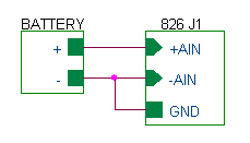
When measuring an unreferenced voltage source such as a battery or isolated power supply, or a sensor powered by such sources, connect the signal ground to GND to avoid high CMV. GND may be connected to either +AIN or -AIN.
IC temperature sensor
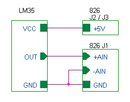
This circuit uses an LM35 integrated circuit to measure temperature. 5 V is routed from the J2 or J3 connector to power the IC. GND is connected to -AIN because it is the reference for +AIN. The LM35 output voltage is 10 mV/°C, which gives a measurement resolution of better than 0.002 °C on the ±1V measurement range.
Potentiometer position detector
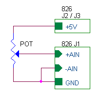
In this circuit, the potentiometer wiper position can be determined by measuring the wiper voltage. Use a linear taper pot to get consistent measurement resolution over the full operating range. For improved accuracy, use a second AIN channel to measure the 5V excitation voltage (as in the thermistor example below).
Precision thermistor measurement
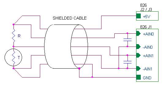
Two AIN channels are used in this circuit, one to measure thermistor voltage (AIN1) and another to measure the 5 V excitation (AIN0). This allows the software to compensate for excitation variations, which is done by computing the ratio of AIN1/AIN0 and then converting the ratio to temperature units. The cable shield should only be terminated at one end, to avoid ground loops. Choose R to obtain the desired measurement resolution.
Isolated sensors
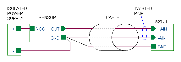
Sensors which are powered by batteries and isolated power supplies can be directly connected to AIN. Connect 826 GND to sensor GND to avoid high CMV. For best performance and accuracy, sense GND at the sensor (by running a dedicated wire from sensor GND to -AIN), and use a twisted pair to reduce common mode noise.
Mitigating high CMV
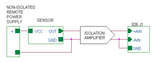
In cases where the CMV would exceed the AIN absolute maximum rating, an isolation amplifier can be used to eliminate the excessive CMV.
Programming basics
- 1. Assign slots
Each analog measurement requires one timeslot (a "slot"). There are 16 slots (numbered 0 to 15), so you can perform up to 16 measurements in a conversion burst.
Start by assigning a slot number to each measurement. It's not required to use all slots, and it's permissible to leave gaps between used slots. For example, you could use only slots 0, 5 and 11 if desired, although it's usually simpler to just use consecutive slots.
- 2. Configure slots
For every slot you assigned, call S826_AdcSlotConfigWrite to configure the slot for the desired analog input channel (AIN), input range and settling time.
IMPORTANT:
You must call S826_AdcSlotConfigWrite once for each slot you are using. Unconfigured slots will measure AIN0 by default.
Each slot can be used to measure any input channel. For example, the following will configure slot 0 to measure AIN13 using the ±10 V range, with 30 µs delay between input switching and start of conversion:
S826_AdcSlotConfigWrite(board, 0, 13, 30, S826_ADC_GAIN_1); // slot 0: measure AIN13 on ±10V range; tsettle = 30µs
- 3. Enable slots
Call S826_AdcSlotlistWrite to enable all of the slots you are using. The second argument is a set of flags in which each bit is associated with a particular slot (bit 0 = slot 0, bit 1 = slot 1, etc.): '1' enables the slot and '0' disables it. For example, if you are only using slot 0 (e.g., as shown above, to measure AIN13):
S826_AdcSlotlistWrite(board, 0x0001, S826_BITWRITE); // enable only slot 0
If instead you were using slots 0, 1 and 15, you would do this:
S826_AdcSlotlistWrite(board, 0x8003, S826_BITWRITE); // enable slots 0, 1 and 15
Or if using all slots, do this:
S826_AdcSlotlistWrite(board, 0xFFFF, S826_BITWRITE); // enable all slots (0 to 15)
Note: You can call S826_AdcSlotlistWrite while the ADC is running to dynamically enable/disable particular slots.
- 4. Select trigger mode.
Use Continuous Mode if you want conversions to run automatically (disables hardware triggering):
S826_AdcTrigModeWrite(board, 0); // trigger mode = continuous
- 5. Start ADC conversions
S826_AdcEnableWrite(board, 1); // start adc conversions
- 6. Read ADC data
Call S826_AdcRead to receive ADC samples. Note that within each sample, the binary ADC data is the least-significant 16 bits. For example, to read a sample from only slot 0:
int samples[16];         // adc samples -- Note: buffer must always be sized for 16 slots
uint slotlist = 0x0001;  // read slot 0
S826_AdcRead(0, samples, NULL, &slotlist, S826_WAIT_INFINITE); // get adc data
printf("Binary adc data = %d", samples[0] & 0xFFFF);
Or you could do this to read all slots:
int samples[16];         // adc samples
uint slotlist = 0xFFFF;  // read all slots
S826_AdcRead(0, samples, NULL, &slotlist, S826_WAIT_INFINITE); // get adc data
for (int i = 0; i < 16; i++)
  printf("AIN%d binary adc data = %d"\n, i, samples[i] & 0xFFFF);
Converting ADC data to volts
This function converts an ADC sample to volts:
double GetAdcVolts(int sample, uint range)  // note: assumes valid range
{
  short adcdata = (short)(sample & 0xFFFF); // extract binary adc data from sample
  double frac = adcdata * (1.0 / 0x7FFF);
  switch (range) {
    case S826_ADC_GAIN_10: return frac;        break;  // -1V to +1V
    case S826_ADC_GAIN_5:  return frac * 2.0;  break;  // -2V to +2V
    case S826_ADC_GAIN_2:  return frac * 5.0;  break;  // -5V to +5V
    case S826_ADC_GAIN_1:  return frac * 10.0; break;  // -10V to +10V
  }
}
Example usage:
int samples[16];         // adc sample buffer
uint slotlist = 0x0001;  // only slot 0 is used in this example
S826_AdcRead(0, samples, NULL, &slotlist, S826_WAIT_INFINITE); // acquire sample
printf("ADC measured %f volts", GetAdcVolts(samples[0], S826_ADC_GAIN_1));
Handling ADC interrupts
An interrupt request (IRQ) is generated when the ADC completes a conversion burst. These IRQs are managed by the blocking function S826_AdcRead, which configures ADC interrupts and handles the resulting IRQs as required. To wait for the next IRQ, simply call S826_AdcRead; the function will return when ADC data is available, and will block and allow other threads to run while ADC data is unavailable.
The following example shows how this works. In this example, only slot 0 is being used, and timestamps are not used. Note that the ADC (and its trigger source) must have been previously configured and enabled (see next example).
void AdcHandler(void)
{
  int errcode;
  int adcdata[16];  // buffer must be sized for 16 slots
  while (1) {
    uint slotlist = 1;  // only slot 0 is of interest in this example
    errcode = S826_AdcRead(0, adcdata, NULL, &slotlist, S826_WAIT_INFINITE); // wait for IRQ
    if (errcode != S826_ERR_OK)
      break;
    printf("Raw adc data = %d", adcdata[0] & 0xFFFF);
  }
}
Periodic ADC conversions (self-paced)
- Can the ADC periodically acquire samples without using a counter to pace it?
Yes: To do this, configure the ADC for continuous triggering mode and use the slot settling times to control the sampling rate. Note that the sampling period will have a small amount of jitter (≤ 1 µs) because ADC conversion time is 2-3 µs. This example shows how to acquire approximately 20 samples per second from analog input 0:
#define SAMPLING_PERIOD 50000         // Sampling period in microseconds (50000 = 20 samples/s).
#define TSETTLE SAMPLING_PERIOD - 3;  // Compensate for nominal ADC conversion time.

// Configure the ADC subsystem and start it running
S826_AdcSlotConfigWrite(board, 0, 0, TSETTLE, S826_ADC_GAIN_1); // measuring ain 0 on slot 0
S826_AdcSlotlistWrite(board, 1, S826_BITWRITE);                 // enable slot 0
S826_AdcTrigModeWrite(board, 0);                                // trigger mode = continuous
S826_AdcEnableWrite(board, 1);                                  // start adc conversions

while (1) {
  AdcHandler();   // Handle periodic ADC interrupts (using code from earlier example)
}
Periodic ADC conversions (using counter)
A counter can be used to periodically trigger ADC bursts. To do this, configure the counter as a periodic timer that outputs a pulse at the end of each period. The output pulse need not be routed to a DIO pin because the board can internally route it directly to the ADC's trigger input. Also, it's not necessary to generate counter snapshots because the ADC will notify software when a conversion burst has completed.
The following code shows how to digitize all 16 analog inputs in a burst, at a rate of period µs/burst. The bursts are triggered by counter0.
// Use counter0 to periodically trigger ADC conversions -------------

void StartAdc16(uint period)  // Configure/start ADC and trigger generator
{
  int i;
  for (i = 0; i < 16; i++)  // Configure all timeslots: 1 slot per AIN; 20µs/slot settling time.
    S826_AdcSlotConfigWrite(0, i, i, 20, S826_ADC_GAIN_1);
  S826_AdcSlotlistWrite(0, 0xFFFF, S826_BITWRITE); // Enable all 16 timeslots.
  S826_AdcTrigModeWrite(0, 0xB0);                  // Hardware triggered, source = counter0 ExtOut.
  S826_AdcEnableWrite(0, 1);                       // Enable ADC conversions.
  CreateHwTimer(0, 0, period);                     // Create and start the trigger generator.
}

int ReadAdc16(int *adcbuf)
{
  uint slotlist = 0xFFFF;     // Wait for ADC burst completion.
  return S826_AdcRead(0, adcbuf, NULL, &slotlist, S826_WAIT_INFINITE);
}
In the following example, all 16 AINs are digitized and processed ten times per second.
int adcbuf[16];       // sample buffer -- always set size=16 (even if fewer samples needed)
StartAdc16(100000);   // Configure adc; start adc and trigger generator (trig every 100K us).
while (ReadAdc16(adcbuf) == S826_ERR_OK) {    // Repeat forever:
  // TODO: PROCESS ADC SAMPLES
}
Oversampling
Oversampling is a useful technique for reducing noise and increasing resolution. Model 826 facilitates oversampling by allowing an analog input (AIN) to be measured multiple times in a single ADC burst. After the burst, the samples can be averaged to obtain an enhanced sample value.
- Example
The following code shows how to oversample two AINs. In each burst, AIN0 is digitized eight times and then AIN1 is digitized eight times. To set this up, each AIN is assigned to eight contiguous slots. For each AIN, the first slot includes a settling time because the ADC input has just switched. The seven subsequent slots do not require settling time (and thus settling times are set to 0 µs) because the input has not switched.
The ADC's internal timing is used to pace conversions, by selecting the continuous triggering mode and assigning appropriate settling times. Slot 0 is assigned a long settling time, which effectively determines the sampling period and also provides a necessary settling delay. Slot 8 has a shorter settling time because it only needs to delay long enough for signal settling.
Note that error checking has been omitted here for clarity, but should always be included in robust application code.
// Settling times in microseconds
#define TSETTLE0 10000  // Delay after switching to AIN0 (tweak this to adjust sampling rate).
#define TSETTLE1 20     // Delay after switching ADC to AIN1.

// Average 8 samples and convert to volts (assumes +/-10V measurement range)
#define VOLTS(SUM)  ((SUM) * 10.0 / (8.0 * 32768.0))

int slot;
int adcbuf[16];  // Sample buffer -- always set size=16 (even if fewer samples needed)

// Adc timeslot attributes.
struct SLOTATTR {
  uint chan;      // analog input channel
  uint tsettle;   // settling time in microseconds
} attr[16] = {                                             // During each burst:
  {0, TSETTLE0},                                           //  switch to AIN0, delay, then digitize
  {0, 0}, {0, 0}, {0, 0}, {0, 0}, {0, 0}, {0, 0}, {0, 0},  //  digitize AIN0 7 more times without delay
  {1, TSETTLE1},                                           //  switch to AIN1, delay, then digitize
  {1, 0}, {1, 0}, {1, 0}, {1, 0}, {1, 0}, {1, 0}, {1, 0}}; //  digitize AIN1 7 more times without delay

// Configure all 16 timeslots.
for (slot = 0; slot < 16; slot++)
  S826_AdcSlotConfigWrite(board, slot, attr[slot].chan, attr[slot].tsettle, S826_ADC_GAIN_1);

// Configure adc system and start it running.
S826_AdcSlotlistWrite(board, 0xFFFF, S826_BITWRITE);  // Enable all 16 timeslots.
S826_AdcTrigModeWrite(board, 0);                      // Select continuous triggering mode.
S826_AdcEnableWrite(board, 1);                        // Start conversions.

while (1)    // Repeatedly fetch and display oversampled data:
{
  int sum[] = {0, 0};                                 // Reset sample accumulators (one per AIN).
  uint slotlist = 0xFFFF;                             // Wait for ADC burst
  S826_AdcRead(board, adcbuf, NULL, &slotlist, 1000); //   and read samples from 16 slots.

  for (slot = 0; slot < 16; slot++)                   // Sum the 8 samples from each AIN
    sum[slot >> 3] += (short)(adcbuf[slot] & 0xFFFF); //   while masking off sample meta-data.

  // Compute and report measured voltages.
  printf("AIN0=%3.3fV, AIN1=%3.3fV\n", VOLTS(sum[0]), VOLTS(sum[1]));
}
Polled operation
- How can I read analog inputs as fast as possible?
In event-driven applications, the S826_AdcRead function is allowed to block until ADC samples are available. However, blocking necessarily involves context switching, which introduces overhead. To avoid this overhead, blocking must be disabled. This is done by setting argument tmax=0, which allows the ADC subsystem to be polled without blocking.
- Example
The following code employs polling to acquire data from all 16 AINs. Each call to S826_AdcRead will return immediately, with slotlist bits indicating the AINs that have new samples waiting in adcbuf. If desired, individual samples may be processed when they arrive in adcbuf (each time S826_AdcRead executes), or the program can wait for all 16 AINs and then process them en masse.
In this example a 7 µs settling delay is allowed before each conversion begins. The ADC conversion time is ≤3 µs, so the total time per AIN is ≤10 µs and the burst time for all AINs is ≤160 µs. Note that individual settling times may need adjustment depending on factors such as source impedance and required accuracy.
#define TSETTLE    7        // Settling delay after switching AIN (adjust as necessary).
#define SLOTFLAGS  0xFFFF   // Timeslot flags: use all 16 timeslots.

int i;
int adcbuf[16];  // Sample buffer -- always set size=16 (even if fewer samples needed)

// Configure all timeslots: 1 slot per AIN; constant settling time for all slots.
for (i = 0; i < 16; i++)
  S826_AdcSlotConfigWrite(board, i, i, TSETTLE, S826_ADC_GAIN_1);

// Configure adc system and start it running.
S826_AdcSlotlistWrite(board, SLOTFLAGS, S826_BITWRITE); // Enable all 16 timeslots.
S826_AdcTrigModeWrite(board, 0);                        // Select free-running mode.
S826_AdcEnableWrite(board, 1);                          // Start conversions.

while (1)    // Repeat forever:
{
  uint remaining = SLOTFLAGS;      // timeslots that have not yet been read
  do {
    uint slotlist = remaining;     // Read all available remaining timeslots.
    int errcode = S826_AdcRead(board, adcbuf, NULL, &slotlist, 0); // note: tmax=0
    remaining &= ~slotlist;

    // OPTIONAL: NEWLY ARRIVED SAMPLES MAY BE PROCESSED WHILE WAITING FOR REMAINING SAMPLES

  } while (errcode == S826_ERR_NOTREADY);

  if (errcode != S826_ERR_OK)
    break; // error

  // TODO: PROCESS ALL UNPROCESSED SAMPLES IN ADCBUF
}
Software triggering
Some applications require that ADC conversion bursts be triggered by software. To set this up, configure the ADC for hardware-triggering and select one of the board's virtual digital outputs as the trigger source. The software can then write to the virtual digital output to start an ADC conversion burst. The following code shows how to use virtual digital output 0 as a software-controlled ADC trigger:
#define TSETTLE    7        // Settling delay after switching AIN (in microseconds; adjust as necessary).
#define SLOTFLAGS  0xFFFF   // Timeslot flags: use all 16 timeslots.
#define VIRTOUT    0        // Use virtual digital output 0 as ADC burst trigger.

void InitAdc(uint board)
{
  // Configure all timeslots: 1 slot per AIN; constant settling time for all slots.
  int i;
  for (i = 0; i < 16; i++)
    S826_AdcSlotConfigWrite(board, i, i, TSETTLE, S826_ADC_GAIN_1);

  // Configure adc system and start it running.
  S826_AdcSlotlistWrite(board, SLOTFLAGS, S826_BITWRITE); // Enable all 16 timeslots.
  S826_AdcTrigModeWrite(board, VIRTOUT + 182);            // Use virtual digital output as trigger.
  S826_AdcEnableWrite(board, 1);                          // Enable conversions.
}
This triggers a conversion burst:
void TriggerBurst(uint board)
{
  S826_VirtualWrite(board, 1 << VIRTOUT, S826_BITSET);   // Rising edge of trigger starts conversion.
  S826_VirtualWrite(board, 1 << VIRTOUT, S826_BITCLR);   // Falling edge of trigger pulse.
}
This returns True if a conversion burst has completed:
int IsBurstDone(uint board)
{
  uint status;
  S826_StatusRead(board, &status);
  return (status == SLOTFLAGS);
}
This example demonstrates how to use the above code:
InitAdc(0);
while (1)    // Repeat forever:
{
  uint slotlist;
  int slot;
  int adcbuf[16];  // Sample buffer -- always set size=16 (even if fewer samples needed)

  TriggerBurst(0);                      // Trigger a conversion burst.
  do {} while (!IsBurstDone(0));        // Poll until burst completes.
  slotlist = SLOTFLAGS;                 // Copy ADC data into adcbuf.
  int errcode = S826_AdcRead(0, adcbuf, NULL, &slotlist, 0); // note: tmax=0

  for (slot = 0; slot < 16; slot++)    // Display all samples.
    printf("Slot %d sample value = %d\n", slot, adcbuf[slot]);
}
Calibration errors caused by missing shunt
On 826 SDKs earlier than version 3.2.0, analog calibration values will not be applied without J6 (labeled "Calibration Enable") installed. A missing shunt is intended to protect against accidental overwriting of calibration values, but in these SDKs it also prevents the reading of those values. This is resolved in SDK version 3.2.0 and above; in these versions the shunt functions as intended and must be installed only when calibrating the board (though leaving it installed all the time is okay).
If board calibration is incorrect, make sure J6 is installed or upgrade to SDK version 3.2.0 or higher. The 826 SDK can be downloaded from the 826 product page.
ADC transfer functions
Each ADC input voltage range extends slightly beyond the negative end of its indicated range:
| Range: | ±10V | ±5V | ±2V | ±1V |
|---|---|---|---|---|
| ADC data | Input voltage (V) | |||
| 0x7FFF | +10.0 | +5.0 | +2.0 | +1.0 |
| 0x0000 | 0.0 | 0.0 | 0.0 | 0.0 |
| 0x8001 | -10.0 | -5.0 | -2.0 | -1.0 |
| 0x8000 | -10.0003 | -5.00015 | -2.00006 | -1.00003 |
ADC accuracy specification
Resolution and no missing codes are both 16 bits minimum.
| Parameter | Value | Units | Description | ||
|---|---|---|---|---|---|
| Min | Typ | Max | |||
| Integral Nonlinearity Error | ±0.75 | ±1.5 | LSB | Deviation of ADC transfer function from best-fit line | |
| Differential Nonlinearity Error | ±0.5 | ±1.25 | LSB | Deviation of ADC code width from ideal code width | |
| Gain Error | ±2 | ±40 | LSB | Deviation of difference between actual level of last data transition and actual level of first transition from difference between ideal levels | |
| Gain Error Temperature Drift | ±0.3 | ppm/°C | |||
| Zero Error | ±0.8 | mV | Difference between ideal midscale voltage and actual voltage producing the midscale output code | ||
| Zero Temperature Drift | ±0.3 | ppm/°C | |||
Maximum input voltage
The analog inputs accept common mode voltages (CMV) up to ±12V with no resulting input current or damage. CMV up to ±25V is tolerated continuously, though this will cause currents to flow in the analog inputs. CMV greater than 25V may be tolerated for brief intervals, but this can cause significant currents to flow in the analog inputs and is not specified nor guaranteed to be safe.
IMPORTANT: Analog inputs are not isolated
The input CMV is referenced to the GND signal on connector J1, which is internally connected to the PCIe power supply return.
