Difference between revisions of "826 DIOs"
(→Controlling high-power loads) |
|||
| (5 intermediate revisions by one user not shown) | |||
| Line 1: | Line 1: | ||
| + | This page contains application notes and other information about the Model 826 general purpose digital I/O system. | ||
| + | |||
| + | For other 826-related topics, please go to the [[826|top-level 826 page]]. | ||
| + | |||
| + | ==Connector pinouts== | ||
| + | |||
| + | <gallery heights=350px widths=180px> | ||
| + | File:826 pinout J2.gif | ||
| + | File:826 pinout J3.gif | ||
| + | </gallery> | ||
| + | |||
==Connections== | ==Connections== | ||
| Line 30: | Line 41: | ||
====Unreferenced 5V or 3.3V input==== | ====Unreferenced 5V or 3.3V input==== | ||
| − | This circuit can be used to monitor an unreferenced 5V or 3.3V logic signal. The signal ground is tied to 826 GND to keep it from floating. | + | This circuit can be used to monitor an unreferenced 5V or 3.3V logic signal. The signal ground is tied to 826 GND to keep it from floating. In the case of 3.3V logic levels, note that the DIO pin has an internal pull-up to +5V, which may affect the logic-high voltage if the source impedance is high. |
[[File:DioIsolated5V.gif|left|]] | [[File:DioIsolated5V.gif|left|]] | ||
{{Clear}} | {{Clear}} | ||
| Line 51: | Line 62: | ||
====RS-422 inputs==== | ====RS-422 inputs==== | ||
| − | DIO channels are single-ended and therefore | + | DIO channels are single-ended and therefore incompatible with differential RS-422. It is recommended to use an external RS-422 line receiver or optocoupler to produce a TTL/CMOS compatible signal. Alternatively, if you have a spare counter channel then it may be possible to [[826 counters#Encoder FAULT output|use a counter to monitor an RS-422 pair]]. |
| − | ==Programming basics== | + | ==Programming== |
| + | |||
| + | ===Programming basics=== | ||
To unconditionally program all DIO outputs, call <code>S826_DioOutputWrite</code> with the <code>mode</code> argument set to <code>S826_BITWRITE</code> (zero). For example, this code will turn on all DIOs: | To unconditionally program all DIO outputs, call <code>S826_DioOutputWrite</code> with the <code>mode</code> argument set to <code>S826_BITWRITE</code> (zero). For example, this code will turn on all DIOs: | ||
| Line 83: | Line 96: | ||
printf("dio%d = %d\n", i, (pins[1] >> (i - 24)) & 1); | printf("dio%d = %d\n", i, (pins[1] >> (i - 24)) & 1); | ||
| − | ==Setting and clearing DIOs== | + | ===Setting and clearing DIOs=== |
Sometimes it's necessary to set or clear particular DIOs without disturbing others. Typically, this is accomplished with a ''read-modify-write'' (RMW) sequence consisting of reading all DIOs into a buffer, modifying the buffer, and then writing the buffer back to the DIOs. This task is further complicated when multiple threads control the DIOs — a common practice in high-performance event-driven applications — because concurrent RMWs on different threads will conflict with each other. To avoid such conflicts, the RMW must be treated as a critical section (e.g., protected by a mutex or semaphore). | Sometimes it's necessary to set or clear particular DIOs without disturbing others. Typically, this is accomplished with a ''read-modify-write'' (RMW) sequence consisting of reading all DIOs into a buffer, modifying the buffer, and then writing the buffer back to the DIOs. This task is further complicated when multiple threads control the DIOs — a common practice in high-performance event-driven applications — because concurrent RMWs on different threads will conflict with each other. To avoid such conflicts, the RMW must be treated as a critical section (e.g., protected by a mutex or semaphore). | ||
| Line 95: | Line 108: | ||
S826_DioOutputWrite(0, maskB, S826_BITCLR); // Clear DIO 24. | S826_DioOutputWrite(0, maskB, S826_BITCLR); // Clear DIO 24. | ||
| − | ==Debouncing inputs== | + | ===Debouncing inputs=== |
[[File:SwitchBounce.png|thumb|Oscilloscope screenshot showing the "bouncing" voltage when a switch turns on]] | [[File:SwitchBounce.png|thumb|Oscilloscope screenshot showing the "bouncing" voltage when a switch turns on]] | ||
| Line 109: | Line 122: | ||
S826_DioFilterWrite(0, tfilt, enabs); // Activate the DIO filters. | S826_DioFilterWrite(0, tfilt, enabs); // Activate the DIO filters. | ||
| − | ==Edge detection== | + | ===Edge detection=== |
Event-driven software often must execute code in response to DIO input changes (e.g., when a pushbutton is pressed, a photoelectric sensor is activated, etc.). Polling is not a good way to detect these events because it degrades system responsiveness and tends to make the source code convoluted and difficult to maintain. However, the alternative — using interrupts — can complicate and prolong program development. | Event-driven software often must execute code in response to DIO input changes (e.g., when a pushbutton is pressed, a photoelectric sensor is activated, etc.). Polling is not a good way to detect these events because it degrades system responsiveness and tends to make the source code convoluted and difficult to maintain. However, the alternative — using interrupts — can complicate and prolong program development. | ||
| Line 125: | Line 138: | ||
WaitForDioFallingEdge(0, 29); // Example usage: wait for falling edge on dio29 of board number 0. | WaitForDioFallingEdge(0, 29); // Example usage: wait for falling edge on dio29 of board number 0. | ||
| − | = | + | ===Generating a burst of pulses=== |
| − | + | ||
| − | + | ||
| − | + | ||
| − | + | ||
| − | + | ||
| − | + | ||
| − | + | ||
| − | + | ||
| − | + | ||
| − | + | ||
| − | + | ||
| − | + | ||
| − | + | ||
| − | + | ||
| − | + | ||
| − | + | ||
| − | + | ||
| − | + | ||
| − | + | ||
| − | ==Generating a burst of pulses== | + | |
:''How can I make a DIO go active for 10ms and then inactive for another 10ms, and repeat this five times?'' | :''How can I make a DIO go active for 10ms and then inactive for another 10ms, and repeat this five times?'' | ||
| Line 165: | Line 158: | ||
} | } | ||
| − | ==Example application: I<sup>2</sup>C Emulator== | + | ===Example application: I<sup>2</sup>C Emulator=== |
:''Can I use DIOs to communicate with I<sup>2</sup>C devices?'' | :''Can I use DIOs to communicate with I<sup>2</sup>C devices?'' | ||
| Line 173: | Line 166: | ||
If you need to monitor an I<sup>2</sup>C bus or emulate a slave device, consider [[826 counters#Serial data capture (synchronous)|using a counter to capture synchronous serial data]]. | If you need to monitor an I<sup>2</sup>C bus or emulate a slave device, consider [[826 counters#Serial data capture (synchronous)|using a counter to capture synchronous serial data]]. | ||
| − | ==Relay rack compatibility== | + | ==Other== |
| + | |||
| + | ===Controlling output rise-time with an external pull-up=== | ||
| + | |||
| + | Each DIO has an output driver that actively drives the signal to 0 V in the ''on'' state and is high-impedance in the ''off'' state. In the ''off'' state, the channel's internal 10 KΩ resistor passively pulls up the signal to +5 V. When the output switches to the ''off'' state, this 10 KΩ source resistance (combined with circuit capacitance) stretches the DIO rise time, which delays its transition to logic '1'. If the rise time is too long, it can be shortened by adding an external pull-up resistor (and reducing external capacitance) on the signal net. | ||
| + | |||
| + | The following table shows nominal rise times for unloaded DIO pins. Lower resistance values may be needed to compensate external circuit capacitance, but do not use an external pull-up resistor having less than 220 Ω (to prevent excessive DIO output current). | ||
| + | |||
| + | {| class="wikitable" | ||
| + | ! style="text-align:left;"| External pull-up | ||
| + | ! style="text-align:left;"| DIO rise time | ||
| + | |- | ||
| + | |None | ||
| + | |200 ns | ||
| + | |- | ||
| + | |1.2 KΩ | ||
| + | |20 ns | ||
| + | |- | ||
| + | |680 Ω | ||
| + | |10 ns | ||
| + | |} | ||
| + | |||
| + | ===Relay rack compatibility=== | ||
{{ImportantNote|The DIO circuitry on model 826 is not compatible with 15 or 24 VDC modules. When choosing modules for your relay rack, be sure to select modules that are compatible with 5 VDC logic levels.}} | {{ImportantNote|The DIO circuitry on model 826 is not compatible with 15 or 24 VDC modules. When choosing modules for your relay rack, be sure to select modules that are compatible with 5 VDC logic levels.}} | ||
| Line 189: | Line 204: | ||
* 24 channels: G4PB24 | * 24 channels: G4PB24 | ||
| − | ==Maximum output current== | + | ===Maximum output current=== |
DIOs are subject to two different maximum current limits: individual and group. Each DIO is capable of continuously sinking up to 24 mA; this is the maximum individual current. However, it's not permitted for all DIOs to do this simultaneously because this would exceed the maximum group current. | DIOs are subject to two different maximum current limits: individual and group. Each DIO is capable of continuously sinking up to 24 mA; this is the maximum individual current. However, it's not permitted for all DIOs to do this simultaneously because this would exceed the maximum group current. | ||
Latest revision as of 10:03, 29 January 2021
This page contains application notes and other information about the Model 826 general purpose digital I/O system.
For other 826-related topics, please go to the top-level 826 page.
Contents |
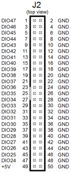
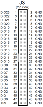
[edit] Connector pinouts
[edit] Connections
IMPORTANT: DIOs are not isolated. An external isolator is required when connecting to a signal which is referenced to a different ground.
DIOs are referenced to the GND pins on connectors J2 and J3, which are internally connected to the PCIe power supply return. When using a DIO to monitor an external signal, make sure the signal is referenced to GND and does not exceed the absolute maximum DIO input voltage range:
- Incompatible signal ground - An optical isolator should be used when connecting to a signal that is referenced to a different ground, or in cases where a ground loop would be created by connecting signal ground to GND.
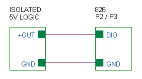
- Unreferenced signal ground - If the signal ground is unreferenced (e.g., the signal generator is powered by an isolated power supply), connect the signal ground to GND. This will reference the external signal to GND.
- Incompatible signal voltage - If the signal is referenced to GND but the signal voltage exceeds the DIO input range, use a level translator or voltage divider to bring it into range. In the latter case, keep in mind that the DIO has an internal pull-up resistor to +5 V.
[edit] 3.3 V compatibility
DIOs are compatible with 3.3 V logic input signals. Note however, that every DIO has an internal 10 KΩ pull-up to +5 V, which can affect the signal voltage from high-impedance 3.3 V sources.
When operating as an output, a DIO produces a high logic level via its internal +5 V pull-up resistor. External 3.3 V circuitry must be 5 V tolerant or must limit the voltage (e.g., with Schottky diode to +3.3 V supply).
[edit] Examples
[edit] Mechanical switch
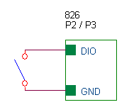
To monitor the state of a mechanical switch, simply connect the switch between the DIO and GND. This takes advantage of the DIO's built-in pull-up resistor.
[edit] Input isolator
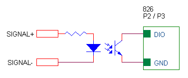
An opto-isolator should be used when the input signal is differential or referenced to a different ground, or in cases where a ground loop would be created by connecting signal ground to GND.
[edit] Unreferenced 5V or 3.3V input
This circuit can be used to monitor an unreferenced 5V or 3.3V logic signal. The signal ground is tied to 826 GND to keep it from floating. In the case of 3.3V logic levels, note that the DIO pin has an internal pull-up to +5V, which may affect the logic-high voltage if the source impedance is high.
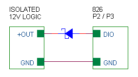
[edit] Unreferenced 12V logic input
Monitoring an unreferenced 12V logic signal. The Schottky diode limits the logic-high voltage applied to the DIO.
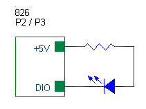
[edit] Driving LEDs
A DIO can directly drive a low-power LED. This is commonly done to light a status indicator or drive an optocoupler. A series resistor is required to limit the LED current. Note that a DIO cannot drive a high-current LED; this requires an external buffer or SSR (see next example).
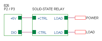
[edit] Controlling high-power loads
A DIO can directly drive many types of solid-state relay. This allows a DIO to control loads that require high voltage, high current or both, such as motors, solenoids, heaters and lighting.
[edit] RS-422 inputs
DIO channels are single-ended and therefore incompatible with differential RS-422. It is recommended to use an external RS-422 line receiver or optocoupler to produce a TTL/CMOS compatible signal. Alternatively, if you have a spare counter channel then it may be possible to use a counter to monitor an RS-422 pair.
[edit] Programming
[edit] Programming basics
To unconditionally program all DIO outputs, call S826_DioOutputWrite with the mode argument set to S826_BITWRITE (zero). For example, this code will turn on all DIOs:
uint dios[] = { // Specify DIOs that are to be turned on (driven to 0 V):
  0x00FFFFFF,   //   DIO 0-23
  0x00FFFFFF    //   DIO 24-47
}
S826_DioOutputWrite(0, dios, S826_BITWRITE); // Turn on all DIOs.
This example shows how to turn on DIOs 7, 13 and 38, and turn off all other DIOs:
uint dios[] = {         // Specify DIOs that are to be turned on:
  (1 << 7) + (1 << 13), //   DIOs 7 & 13 are in first 24-bit mask (DIOs 0-23),
  (1 << (38 - 24))      //   DIO 38 is in second 24-bit mask (DIOs 24-47).
}
S826_DioOutputWrite(0,  // Program all DIO outputs on board 0:
  dios,                 //   desired output states
  S826_BITWRITE);       //   unconditionally change all DIOs
To read the pin levels of all DIOs, call S826_DioInputRead. This example shows how to read and display all DIO pins on board 0:
int i;
uint pins[2];                // Buffer for pin states.
S826_DioInputRead(0, pins);  // Read all DIO pin states into buffer.
for (i = 0; i < 24; i++)     // Display states of DIOs 0-23.
  printf("dio%d = %d\n", i, (pins[0] >> i) & 1);
for (i = 24; i < 48; i++)    // Display states of DIOs 24-47.
  printf("dio%d = %d\n", i, (pins[1] >> (i - 24)) & 1);
[edit] Setting and clearing DIOs
Sometimes it's necessary to set or clear particular DIOs without disturbing others. Typically, this is accomplished with a read-modify-write (RMW) sequence consisting of reading all DIOs into a buffer, modifying the buffer, and then writing the buffer back to the DIOs. This task is further complicated when multiple threads control the DIOs — a common practice in high-performance event-driven applications — because concurrent RMWs on different threads will conflict with each other. To avoid such conflicts, the RMW must be treated as a critical section (e.g., protected by a mutex or semaphore).
Fortunately, the 826 provides a fast, efficient way to set and clear DIOs without the complications of RMW. Simply call S826_DioOutputWrite with the mode argument set to S826_BITSET or S826_BITCLR, as shown in this example:
// Set and clear some DIOs without affecting other DIOs
uint maskA[] = {7, 0};  // bitmask for DIOs 0-2
uint maskB[] = {0, 1};  // bitmask for DIO 24
S826_DioOutputWrite(0, maskA, S826_BITSET);  // Set DIOs 0, 1 and 2.
S826_DioOutputWrite(0, maskB, S826_BITCLR);  // Clear DIO 24.
[edit] Debouncing inputs
DIOs are commonly used to monitor real-world signals that have glitches or other noise. For example, the electrical contacts of mechanical switches may "bounce" when first connected, thus producing pulses that may be incorrectly interpreted by the application program as state changes. This problem can be solved by implementing a software debounce algorithm, but an easier way is to use the input filters provided by the DIO system.
To use the DIO input filters, simply specify a filter interval and designate the DIOs to be filtered. Choose a filter interval that is long enough to suppress the longest expected noise pulse, but not so long that valid state changes will be missed. The following example shows how to suppress pulses up to 200 µs wide on dio0 and dio2:
// Debounce dio0 and dio2 ------------------

#define FILT_USEC 200                  // Desired filter interval (max = 1.31 ms).
uint tfilt = FILT_USEC * 50;           // Interval specified as multiple of 20ns.
uint enabs[] = {5, 0};                 // Enable filters on dio0 and dio2.
S826_DioFilterWrite(0, tfilt, enabs);  // Activate the DIO filters.
[edit] Edge detection
Event-driven software often must execute code in response to DIO input changes (e.g., when a pushbutton is pressed, a photoelectric sensor is activated, etc.). Polling is not a good way to detect these events because it degrades system responsiveness and tends to make the source code convoluted and difficult to maintain. However, the alternative — using interrupts — can complicate and prolong program development.
Fortunately, model 826 provides the best of both worlds: it implements DIO edge detection circuitry with interrupts for efficient event monitoring, and the API makes the interrupts easy to use. For example, the following function will return when a falling edge is detected on a particular DIO. It is a blocking function, meaning that other threads can run while it waits for the DIO edge.
int WaitForDioFallingEdge(uint board, uint dio)
{
  uint rise[] = {0, 0};       // not interested in rising edge
  uint fall[] = {(dio < 24) << (dio % 24), (dio > 23) << (dio % 24)}; // interested in falling edge
  S826_DioCapEnablesWrite(board, rise, fall, S826_BITSET);   // Enable falling edge detection.
  return S826_DioCapRead(board, fall, 0, INFINITE_WAIT);     // Block until falling edge.
}

WaitForDioFallingEdge(0, 29);  // Example usage: wait for falling edge on dio29 of board number 0.
[edit] Generating a burst of pulses
- How can I make a DIO go active for 10ms and then inactive for another 10ms, and repeat this five times?
There are several ways to do this but the methods you can use depend on a number of factors. Here are two approaches:
- If you need precise timing then you can use two counters as shown in High resolution pulse-burst generator.
- If high precision is not needed then you could bit-bang the DIO, using a hardware timer (or system
Sleepfunction) to pace the DIO writes like this:
int i;
uint mask[] = {1, 0};       // bitmask for dio0
CreateTimer(0, 0, 10000);   // Create 10 ms timer and start it running.
for (i = 0; i < 5; i++) {
  WaitForTimer(0, 0);                         // Wait for timer tick.
  S826_DioOutputWrite(0, mask, S826_BITSET);  // Set dio0 active.
  WaitForTimer(0, 0);                         // Wait for timer tick.
  S826_DioOutputWrite(0, mask, S826_BITCLR);  // Set dio0 inactive.
}
[edit] Example application: I2C Emulator
- Can I use DIOs to communicate with I2C devices?
Have a look at Sensoray's I2C emulator, which uses two DIOs to bit-bang an I2C bus. This open source software implements a full-featured I2C master emulator with bus arbitration and bus-hang resolver. All 826-specific code resides in a hardware abstraction layer (HAL) — an architectural feature that belongs in all production-quality software.
If you need to monitor an I2C bus or emulate a slave device, consider using a counter to capture synchronous serial data.
[edit] Other
[edit] Controlling output rise-time with an external pull-up
Each DIO has an output driver that actively drives the signal to 0 V in the on state and is high-impedance in the off state. In the off state, the channel's internal 10 KΩ resistor passively pulls up the signal to +5 V. When the output switches to the off state, this 10 KΩ source resistance (combined with circuit capacitance) stretches the DIO rise time, which delays its transition to logic '1'. If the rise time is too long, it can be shortened by adding an external pull-up resistor (and reducing external capacitance) on the signal net.
The following table shows nominal rise times for unloaded DIO pins. Lower resistance values may be needed to compensate external circuit capacitance, but do not use an external pull-up resistor having less than 220 Ω (to prevent excessive DIO output current).
| External pull-up | DIO rise time |
|---|---|
| None | 200 ns |
| 1.2 KΩ | 20 ns |
| 680 Ω | 10 ns |
[edit] Relay rack compatibility
IMPORTANT: The DIO circuitry on model 826 is not compatible with 15 or 24 VDC modules. When choosing modules for your relay rack, be sure to select modules that are compatible with 5 VDC logic levels.
Each 50-pin DIO header carries 24 DIO signals that have 5 V logic levels. The header pinout is compatible with the following module racks and other racks that have the same pinouts:
Grayhill (various module types):
- 8 channels: 70RCK8-HL, 70MRCK8-HL, 70GRCK8-HL, 70LRCK8-HL, 70RCK8-DIN
- 16 channels: 70RCK16-HL, 70MRCK16-HL, 70GRCK16-HL, 70LRCK16-HL, 70RCK16-DIN
- 24 channels: 70MRCK24-HL, 70LRCK24-HL, 70LRCK24-DIN
Opto-22 (type G4 modules):
- 8 channels: G4PB8
- 16 channels: G4PB16
- 24 channels: G4PB24
[edit] Maximum output current
DIOs are subject to two different maximum current limits: individual and group. Each DIO is capable of continuously sinking up to 24 mA; this is the maximum individual current. However, it's not permitted for all DIOs to do this simultaneously because this would exceed the maximum group current.
DIO channels are organized into groups as shown below. In any particular group, the group current is the total of all individual currents in the group. For example, in Group4 the group current is the sum of the currents flowing in DIO24 through DIO29.
| Group | DIOs |
|---|---|
| 0 | 0-5 |
| 1 | 6-11 |
| 2 | 12-17 |
| 3 | 18-23 |
| 4 | 24-29 |
| 5 | 30-35 |
| 6 | 36-41 |
| 7 | 42-47 |
Each group is capable of continuously sinking up to 72 mA. As shown in the following table, all DIOs in a group may be active at the same time if their individual currents are less than or equal to 12 mA (because 6 * 12 ≤ 72). However, when the individual currents are higher than 12 mA, it is not allowed for all DIOs in a group to be active at the same time.
| DIO current (mA) | Maximum number of active DIOs |
|---|---|
| i ≤ 12 | 6 |
| 12 < i ≤ 14.4 | 5 |
| 14.4 < i ≤ 18 | 4 |
| 18 < i ≤ 24 | 3 |
